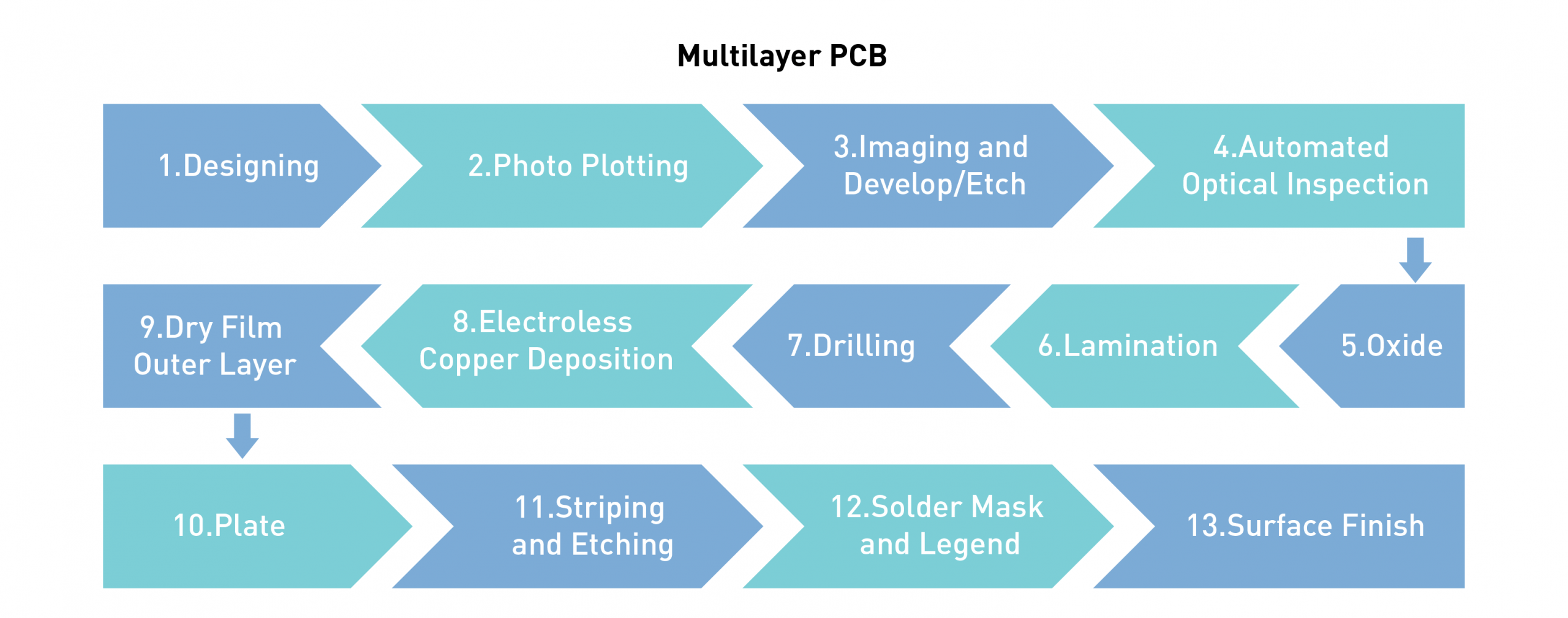
Multilayer Pcb Manufacturing Process Steps

What Are The Steps In The Pcb Assembly Process Printed Circuit Boards Printed Circuit Circuit Board

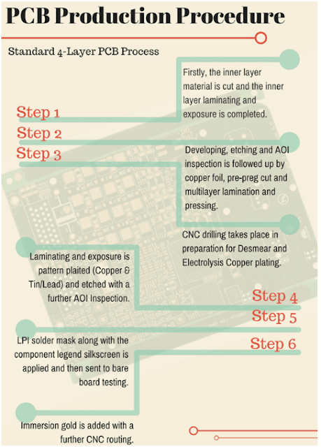
A Guide To The Pcb Manufacturing Process Mcl
Pcb Manufacturing Process News Season Multilayer Circuit Shenzhen Co Ltd

How Multilayer Pcb Manufacturing Is Different From Single Layer Pcb Manufacturing
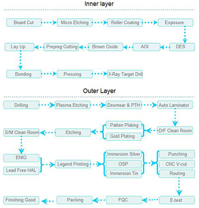
Multilayer Pcb Manufacturing Process A Tech Circuits
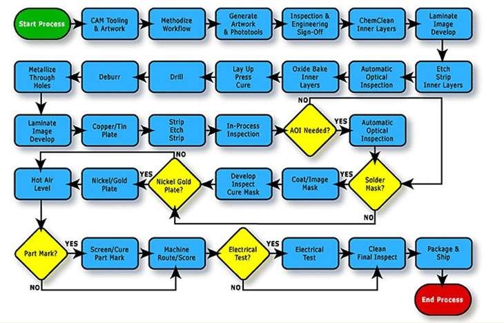
Mass Pcb Production Process Aipcba

Because it is made by electronic printing it is called printed circuit board.
Multilayer pcb manufacturing process steps.

Pcb With Blind And Buried Vias Blinds Bury Printed Circuit Board
How To Manufacture Multilayer Pcb Moko Technology

Pcb Manufacturing Process How Are Pcb Made Process Flowchart

Ro4003rogers Fr4 Mix Laminate Multilayer Pcb With Step Design Steps Design Pcb Circuit Board Multi Layering

Single Double Sided Pth Pcbs From Clarydon

Ipc 2226 Standard For Hdi Pcb Design Hdi Board Manufacturer Pcb Design Circuit Board Printed Circuit Board

Pin On Printed Circuit Board

Pcb Fabrication Process What Are The Pcb Manufacturing Process Steps

Pin On Production Process

The Top Layout Software For Pcb Design Output Files Printed Circuit Board Appliance Sale Appliance Warehouse

A Multi Layer Pcb Requires A Number Of Reliable Processes To Make Copper Layer With More Than 3 Oz In Thickness Manufacturing Multi Layering China

Ipc 2226 Standard For Hdi Pcb Design Hdi Board Manufacturer Pcb Design Circuit Board Printed Circuit Board

Ipc 2226 Standard For Hdi Pcb Design Hdi Board Manufacturer Pcb Design Printed Circuit Board Circuit Board

Resist Strip In 2020 Common Phrases How To Remove Circuit Board

Pcb Documentation Notes You Shouldn T Miss Miracle Aerospace Notes Documents Miracles

Knowledge Of Pcb Impedance Control Printed Circuit Boards Circuit Board Design Printed Circuit Board

Market Research On Global And Chinese Printed Circuit Board Pcb Industry Analysis Research Repor Circuit Board Design Circuit Design Printed Circuit Board

Picking Advanced Multilayer Pcb Online With Images Circuit Board Design Circuit Board Printed Circuit Board
Https Encrypted Tbn0 Gstatic Com Images Q Tbn 3aand9gctnicpetgykewf54euuo9qn74idlvv5msu78krdh Xodopb2yg6 Usqp Cau

Printed Circuit Board Prototype With Images Circuit Board Printed Circuit Printed Circuit Board

Desmear In 2020 Printed Circuit Board Fabric Turn Ons

Pcb Board Manufacturing Pcb Prototyping Service Pcb Assembling Services Rayming Tech 6 Layer Security Products Printed Circuit Board Circuit Board Circuit
Http Www Panda Pcb Com Flexible Pcb Or Fpc Or Call Flexible Circuit Technology Opens The Window To New Opportunitie Flex Circuit Board Printed Circuit Board

Spi Laser Inverter Circuit Board Buy Online In 2020 Circuit Board Electronics Circuit Circuit

Pcb Pics Printed Circuit Boards Circuit Board Pcb Board

Quick Prototyping Solutions Circuit Cellar

Hasl Pcb With Images Electronic Components Logic Board Electronics

Infographics 6 Layer Of Pcb Fabrication Production Process Greatpcb Smt Limited

Multi Layer Pcb In 2020 Printed Circuit Board Printed Circuit Boards Circuit Board

2 Layer Rigid Pcb Posted Today Circuit Board Printed Circuit Board Surface Finish

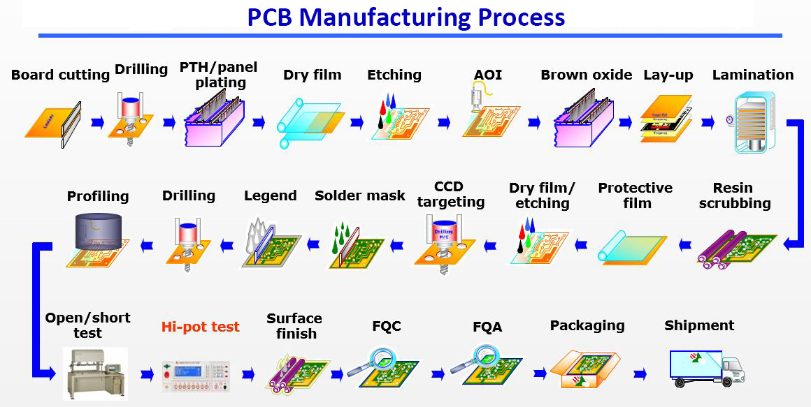
Complete Manufacturing Process Flow Diagram Pcb Manufacturing Process Flow In 2020 Process Flow Diagram Process Flow Process Flow Chart

Choosing China Pcb Manufacturer Online Printed Circuit Board Circuit Board Printed Circuit

Pin On Production Process

94v2 Pcb Circuit Board Pcb Circuit Board Circuit Board Printed Circuit Board

Micro Via Pcb Multilayer Pcb Printed Circuit Board Circuit Board Printed Circuit

Pcb Manufacturer Manufacturing Layer Mask Sale
6 Amazing Pcb Fabrication Process Greatpcb Smt Limited

Pcb Assembly Is It Good To Outsource Miracle Aerospace Party Expert Assembly Aerospace

A Day In The Life Of A Pcb Manufacturing Process Altium Pcb Design Software

Pin By Smith On Mcpcb Pcb Board Unique Boards

Pin By Hebei Chenfei Electronic Tech On The New Pcb Boards Pcb Board Manufacturing Electronics

Pin On Production Process

Dfm Mistakes In Printed Circuit Board Circuit Board Design Printed Circuit Board Circuit Board
Https Encrypted Tbn0 Gstatic Com Images Q Tbn 3aand9gcrrcbuzwfko3qqzq Hpjcnpdxetns4zm8icevq990o Rdptmrzy Usqp Cau
Source : pinterest.com
